Latest Blog
UV laser drilling of SiC for semiconductor device fabrication
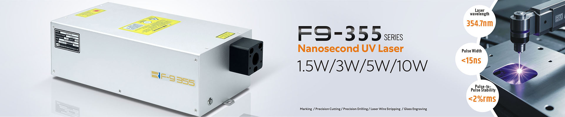
Apr 19 , 2021Pulsed UV laser processing is used to drill micro holes in silicon carbide (SiC) wafers supporting AlGaN/GaN transistor structures. Direct laser ablation using nanosecond pulses has been proven to provide an efficient way to create through and blind holes in 400 µm thick SiC. When drilling through, openings in the front pads are formed, while blind holes stop ~40 µm before the backside and were advanced to the electrical contact pad by subsequent plasma etching without an additional mask. Low induction connections (vias) between the transistor's source pads and the ground on the backside were formed by metallization of the holes. Micro vias having aspect ratios of 5-6 have been processed in 400 µm SiC. The process flow from wafer layout to laser drilling is available including an automated beam alignment that allows a positioning accuracy of ±1 µm with respect to existing patterns on the wafer. As proven by electrical dc and rf measurements the laser-assisted via technologies have successfully been implemented into fabrication of AlGaN/GaN high-power transistors.