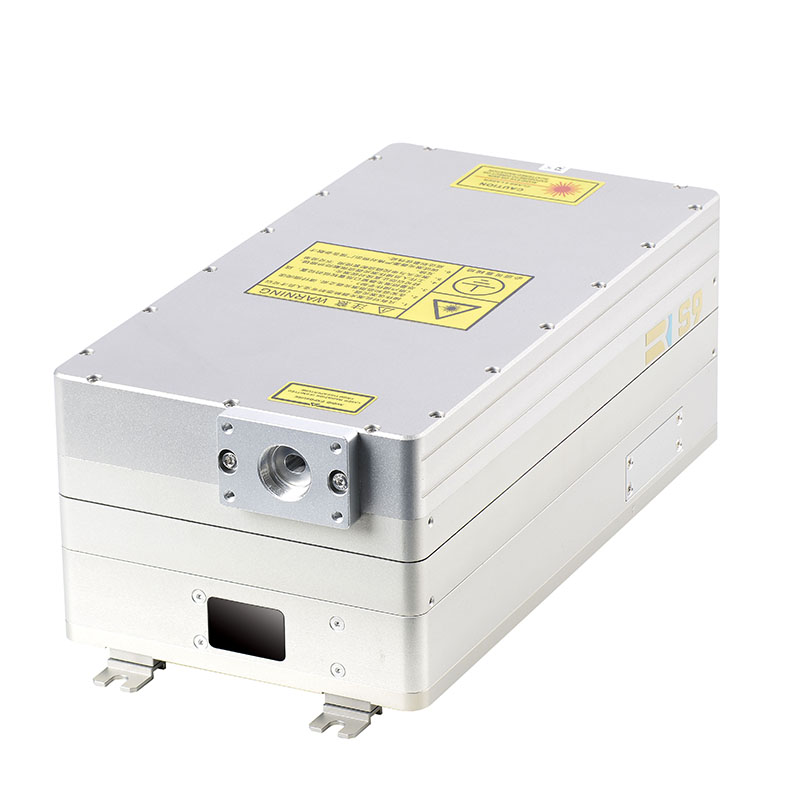
uv Laser systems for wafer serialization, marking and scribing
Apr 27 , 2021Semiconductor wafer processing typically requires serialization, patterning and roughening operations. And picking the correct laser system for these operations can be complex once you consider all the relevant process variables—such as substrate type, wafer diameter, feature size, slag tolerances, debris volume, throughput and clean room protocols.
Whether marking or cutting wafers, lasers bring distinct advantages and cost savings to semiconductor manufacturing. The non-contact and low-residual processes are necessary in marking everything from blank silicon wafers to completed, packaged devices.
CMS Laser’s wafer processing systems offer a wide range of solutions including serialization for traceability, scribing and lapping. Our laser systems can process the full range of semiconductor substrates and coatings—include silicon, sapphire, lithium tantalate, silicon carbide, III-V semiconductors, II-VI semiconductors, and photo resists.
Our engineers understand the nuances of wafer handling, throughput and clean room requirements. They have experience with a wide variety of substrate types—silicon, sapphire, GaAS, InP, SiGe and more.
We can tailor turnkey laser systems to your application requirements, accounting for geometric, dimensional, line width and slag tolerances.
