Latest Blog
355nm UV laser cold processing of silicon wafer microvias and blind holes
Jul 24 , 2023When it comes to 355nm UV laser cold processing of silicon wafer microvias and blind holes, there are several important factors to consider.
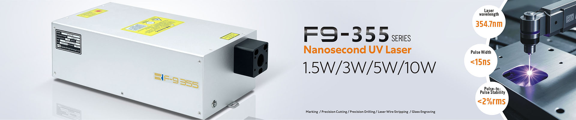
Firstly, the 355nm UV laser is a type of ultraviolet laser that operates at a wavelength of 355 nanometers. This wavelength is particularly well-suited for processing silicon wafers due to its high absorption by silicon material.
The cold processing aspect refers to the fact that the UV laser does not generate significant heat during the processing of the silicon wafer. This is important because excessive heat can cause damage to the delicate microvias and blind holes present on the wafer.
The UV laser is able to precisely ablate the silicon material, creating microvias and blind holes with high accuracy and minimal thermal damage. This is crucial for the production of advanced electronic devices, as these microvias and blind holes are often used for interconnects and signal routing.
Furthermore, the 355nm UV laser offers several advantages over other laser types, such as fiber lasers. UV lasers have a shorter wavelength, which allows for higher precision and smaller feature sizes. Additionally, the UV laser can be focused to a smaller spot size, enabling finer details in the processing of the silicon wafer.
In conclusion, the 355nm UV laser cold processing of silicon wafer microvias and blind holes is a highly precise and efficient method for manufacturing advanced electronic devices. Its ability to generate minimal heat and its high accuracy make it an ideal choice for this application.


