Application of UV laser cutting machine in semiconductor wafer
May 21 , 2021Application of UV laser cutting machine in semiconductor wafer
In recent years, with the rapid development of the optoelectronic industry, the demand for highly integrated and high-performance semiconductor wafers has continued to grow. Materials such as silicon, silicon carbide, sapphire, glass, and indium phosphide have been widely used as substrate materials for semiconductor wafers. With the substantial increase in wafer integration, wafers tend to be lighter and thinner, and many traditional processing methods are no longer applicable, so laser stealth cutting technology is introduced in some processes.

Laser cutting technology has many unique advantages:
1. Non-contact processing: In laser processing, only the laser beam is in contact with the processed part, and no cutting force acts on the cut part to avoid damage to the surface of the processed material.
2. High processing accuracy and low heat influence: Pulsed laser can achieve extremely high instantaneous power, extremely high energy density and low average power, and can complete processing instantly with extremely small heat-affected area, ensuring high-precision processing and small heat-affected area .
3. High processing efficiency and good economic benefits: The laser processing efficiency is often several times that of the mechanical processing effect and there is no consumables and pollution. The laser stealth cutting technology of semiconductor wafers is a brand-new laser cutting process, which has many advantages such as fast cutting speed, no dust generated during cutting, no loss of cutting substrate, small cutting path required, and complete dry process. The main principle of stealth cutting is to focus the short-pulse laser beam through the surface of the material in the middle of the material, form a modified layer in the middle of the material, and then separate the chips by external pressure.
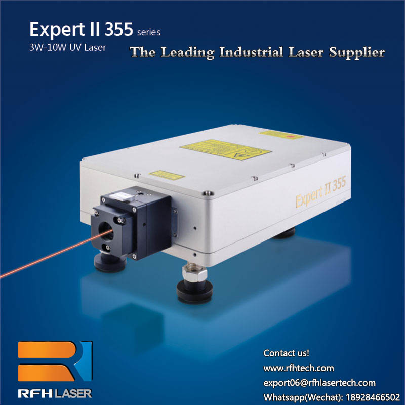
UV laser cutting machines have been widely used in semiconductor integrated circuits, including single and double mesa glass passivation diode wafer dicing, single and double mesa thyristor wafer dicing, gallium arsenide, gallium nitride, IC wafer Cutting dicing.