Latest Blog
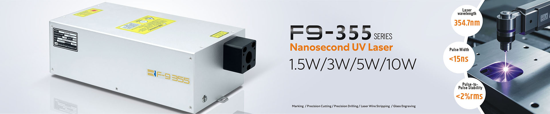
PCB Laser Depanelizing Using a high power UV Laser source 355nm
Feb 06 , 2023PCB Laser Depanelizing Using a high power UV Laser source
One of the methods gaining in popularity for singulating rigid/flex, rigid and flex circuit
boards post assembly is through the use of laser routing. This method has the
advantage of speed, positional accuracy, no tooling wear and lastly no induced
mechanical stresses on components during the singulating process.
There are several cases where laser routing of printed circuit boards is desirable:
o when a high degree of precision of the final assembly is required (think
“tight fit” of a board in to an assembly) or
o when numerous materials need to be cut through and the number and
type of depanelizing steps is to be limited (think “not compromising
cutting one material by using a technique that does not work well on a
second or third material”) or when
o unusual board shapes come up in a design or finally when
o highly sensitive components are placed near the cut out lines of the PCB
need to be treated gingerly.
There are a variety of depaneling options available for PCBs, each with its
own set of advantages and disadvantages.
PCB Depaneling Options
The methods for straight line PCB singulating, which are set up for rectangular-shaped
PCBs, all cut or crush the edge of the board edge. These methods include die cutting,
punching or V-scoring the assembly or by using a wheel cutter or a saw.
The sawing method typically uses a single rotating blade spinning at high RPM to cut
the panel into the shapes required. This method produces heat in the cut out area as
well as creating debris as a byproduct of the cutting operation.
In V-scoring the depth of the thickness of the board is 30-40% of the original board
thickness as it is cut from both sides of the board. After assembly the board is broken
at this v-score line. Alternately a “pizza cutter” cuts through the V-score of the panel
and cuts the remaining web until the boards are in their final cutout shape thereby
putting strain on the components and solder joints-especially those near the board
edge.
In another method, the singulated board outline can be punched out form the panel.
This requires that a new punch be used for every single type of circuit board which
means it is not a flexible method of board cut out. The punch force can also bend or
deform the edges of the PCB. Sharp edges of a well-maintained die must be the norm
in order to get a defect-free cutout.
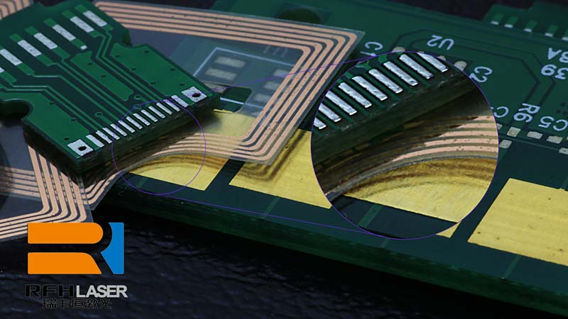
In board routing and subsequent “nibbling” on a board outline can also be
cut out. Boards are routed prior to assembly. The remaining attached
points are drilled with a small drill thereby making it easier to break
the boards out from the panel post board assembly. This leaves socalled “mouse bite” patterns behind. The routing takes up panel space
as there are keep out requirements around the edge of the board cut
out area. The routing can also reduce panel stiffness which is typically
required and desire during the initial stages of the PCB assembly
process. The advantage the routing process is that curved and nonlinear line patterns can be cut using the router bit.
In each of the above techniques, all of which are mechanical in nature, the board
edges, parts near the cut out area as well as the solder joints will have a high degree of
stress placed on them during the cutting process. This stress may cause delamination of
the board near its edges or develop space in and round the glass fibers near the board
edge. Both of these anomalies may lead to moisture ingress in to the board which may
lead to reliability problems down the road. These potential problems enlarge the “keep
out” areas of the components along the periphery of the boards.
Laser Machining Options
There are several methods by which laser machining can be used to create the board
cutout patterns including perforations, hold-in tabs and scoring. The precision of the
laser cutting source allows for much smaller PCB geometries to be singulated. The
precision of the laser is quite tight especially when compared to other mechanical
methods. The C02 laser sources are positionally and dimensionally within 2 mils (50um)
while the UV sources are within 1 mil (25 um)
Perforations
Similar to scoring or v-grooves, laser perforations are another option for tool-less PCB
removal from a panel. Perforations can be laser formed to any size and spacing to meet
the desired removal and securement forces.
Hold-in Tabs
Hold-in tabs are small uncut sections around the board used to secure the board in the
panel. The hold-in tabs are used due to the ease of handling small parts or part
securement for additional processing. The hold-in tab width is chosen based on the
amount of force desired to remove the individual board from the panel/sheet or known
forces to be applied by downstream processes like component loading or electropolishing. The laser can create tabs in most any material and to any width and location
about the board.
Scoring
Laser scoring produces a limited depth ablation line in the board material or materials.
The depth is generally 50% of the material thickness but can be controlled to a desired
depth. The scoring acts similar to the hold-tab to secure the PCB in to the panel, but
allows for individual parts to be 'snapped' out. Laser scoring lines can also be used as a
deliberate path for stress relief or crack propagation.
How 355nm UV lasers function
UV lasers operating at 355nm are used to ablate or to disintegrate the board material. A
high energy laser pulse vaporizes and removes the top layer explosively turning it into
micro dust particles. This requires that the material, whether it be FR-4, polyimide,
metals or some combination thereof needs to be able to absorb the pulse. The laser
beam goes back and forth over the cut through location ablating a little bit at a time.
This means that because only a small amount of material at a time is vaporized, the
local heating effect is minimized. In fact, measurements taken near the cutting area
(within 1.5 mm of the cut area) show that the temperature rise is well below 1000ͦ Cbelow that of the reflow profile (1). While other shorter wavelength lasers may be more
optimal in terms of performance, their use is limited by their high capital requirements
In order to reduce the cut time and the associated expense the laser beam is “beam
steered” using a galvanometer (galvo). This traces the cutting path in the material over
a small area. This scanner approach arrows the beam to be moved at a very high rate
of speed in the same location over a small area. This speed is in the range from 100 to
1000mm/sec. This makes sure that the beam is in the same area for only a short period
of time thereby minimizing local heating affects.
The fiducials of the board can help determine the relative required location of the beam
cutting location. An X-Y precision table is used for larger mechanical movements and
adjustments while the galvo takes on the micro movements and adjustments of
location.
Conclusion
Laser depaneling of PCBs has its application niche where boards have tight spacing,
where geometric tolerances are critical and where the cutout location lines are very
close to components. The method allows for precise cut out of the boards during the
singulation process with very little heating of the board and very little mechanical stress
compared to traditional board depaneling techniques.


