Latest Blog
The difference between Nanosecond Lasers cooled source and PCB dedicated CO2 laser equipment
Jun 27 , 2022The difference between Nanosecond Lasers cooled source and PCB dedicated CO2 laser equipment
The 2020 South China Advanced Laser and Processing Application Technology Exhibition will be held at the Shenzhen International Convention and Exhibition Center (Bao'an New Hall) from November 3 to 5. Under the premise of covering the core resources of the entire industrial chain of electronic intelligent manufacturing, the exhibition will focus on 5G and The theme of new infrastructure, driving new demands, and triggering new scenarios will explore the application of lasers in PCB, lithium battery, consumer electronics, microelectronics, medical and other fields, aiming to bring the audience an updated and more refined laser application exchange platform.
This issue of Radium Sir will take you to know in advance the exhibitors and exhibits that can apply laser processing technology to PCB circuit board processing at the South China Laser Exhibition, as well as their recommended exhibits suitable for PCB circuit board processing. Before visiting the South China Laser Exhibition, you must not miss these fairy companies. ■ TIPS
PCB (Printed Circuit Board), the Chinese name is printed circuit board, also known as printed circuit board, is an important electronic component, electronic component support and electrical connection carrier. Because it is made using electronic printing, it is called a "printed" circuit board.
uv laser | green laser | Ultraviolet lasers | uv dpss laser | nanosecond laser | UV laser source | Solid State Lasers
Almost every electronic device, ranging from electronic watches and calculators, to computers, communication electronic equipment, and military weapon systems, as long as there are electronic component systems with integrated circuits, in order to make electrical interconnections between various components, PCBs are used. plate. In the process of producing PCB boards, in order to improve the efficiency and yield, the processors first produce the whole board in a large area, and then cut it into small pieces during the use process, and the specific and important processing One way is laser processing.
In the past ten years, PCB circuit boards have been increasingly used in the fields of consumer electronics and automotive electronics such as mobile phones. The cutting edge has no dust, no burrs, no deformation, and no edge components are affected. basic requirements. The traditional processing mode often affects the performance of the PCB circuit board to varying degrees, or generates stress, dust and other harmful tiny particles during processing or causes static electricity to affect the performance of the circuit board. In contrast, laser cutting, laser marking and other processes stand out among the many processing modes of PCB boards because of their non-contact processing methods, small processing gaps, and no harmful tiny particles and static electricity. Favored by major PCB manufacturers.
Coherent (Beijing) Commercial Co., Ltd.
- Coherent Inc. -
■ Laser Intelligent Manufacturing Innovation Exhibition Area 12H59
Company Introduction Coherent, founded in 1966, is a world-renowned supplier of lasers and laser technology, serving scientific research, business and industry. Coherent spans the globe and is headquartered in the heart of California-Silicon Valley, providing a unique portfolio of products and services for research, life sciences, microelectronics and materials processing.
Products AVIA LX Lasers
product description
With the continuous development of ultra-thin and miniaturized 3C electronic devices such as smartphones, in order to achieve the goals of less space, faster speed and higher performance, electronic products have a more prominent demand for high-density PCBs. The requirements of "light, thin, short and small" are constantly increasing. In order to achieve this goal, multilayer boards gradually dominate the market, and the circuit layout of the PCB board needs to be closer to the edge of the board. Both of these requirements pose challenges to PCB cutting. How to improve the edge quality of cutting, reduce the heat-affected zone, and reduce the width of the incision while ensuring production capacity and not increasing the cost has become a technical challenge in the PCB processing process.
When using traditional lasers to cut thick plates, it is generally necessary to reserve a V-groove to avoid interruption of the optical path during the cutting process and reduce the laser power and affect the cutting efficiency. When cutting with Coherent's AVIA LX laser, pulse energy up to 400μJ can be fully utilized to scribe repeatedly along the same line, no V-grooving is required, so the cutting speed is faster and the kerf width is significantly reduced.
Features
■ Cost-effective, high-yield, high-efficiency, high-quality and stable
■ Can effectively reduce heat affected zone, improve cutting edge quality, reduce kerf width and increase production
■ AVIA LX works with virtually any existing PCB material, including fiberglass materials
Product advantages
Cut cross-sections of 1.6 mm thick multilayer PCBs with fiberglass layers using a competitor's UV solid-state laser and a Coherent AVIA LX laser, which has narrower trench channels and smaller HAZs.
Top view of a 0.95mm-thick PCB cut using a competitor's UV solid-state laser and Coherent's AVIA LX laser with a narrower, more consistent cut.
For lasers with lower pulse energies, the beam focus must be constantly moved as the beam penetrates the material, so that the minimum size of the focus always precisely matches the depth of cut in order to obtain a laser flux above the material ablation threshold. However, in the actual processing process, it is necessary to move the PCB board, or additionally use a three-axis scanner with focusing function. Either method will greatly affect the overall processing efficiency and schedule, increasing equipment costs and operational complexity.
The AVIA LX utilizes Coherent's advanced laser pulse timing and spatial positioning technology, which avoids heat generation in the substrate to a certain extent, eliminates thermal damage, and allows greater use of the high pulse of the laser when cutting thicker materials. energy. The high pulse energy of AVIA LX increases the laser focusing tolerance of the work surface. During the cutting process, the laser light source only needs to focus on a point in the middle of the PCB; at the same time, the high pulse energy of AVIA LX ensures that there is enough laser flux for ablation, As a result, the cutting speed can be accelerated, and the entire operating system is also very simple and convenient.
Features
Compared with traditional processes, laser PCB board coding has better accuracy and flexibility, which can make up for the shortcomings of traditional process processing, greatly improve production efficiency and yield, reduce costs and reduce pollution.
Applications
At present, it has been widely used in many fields such as digital products, wearable devices, and automotive circuit boards.
Product 1
PCB CO2-FTW055 Flying Marking System
product description
■ The equipment is directly connected to the PCB production line, and can be installed after developing (printing→exposure→developing→on-the-fly coding→post-baking) or other positions, mainly for marking characters. The equipment adopts the flying marking method. The PCB board flows into the equipment through the assembly line, and flows out of the equipment after flying marking. The PCB board does not need to stop during the whole process. Large marking range: 620*730mm. More than 160 groups of characters can be marked at one time (6 characters per group)
Applications
■ Cutting and drilling of hard and brittle materials: glass, sapphire, ceramic
■ Flexible material cutting, drilling: FPC, OLED, LCP
■ Special fine micromachining
Product 2
Large format PCB marking system (CO2-PCB650)
product description
■ It can mark characters, one-dimensional codes, two-dimensional codes and other small carts to automatically load and unload, and the multi-channel independent vacuum adsorption design ensures the stable loading and unloading of porous large boards. High precision, barcode gun automatically calibrates precise XY servo system, stable operation and fast speed
■ Laser configuration: CO2, green light 10W, UV optional
Features
■ Single wavelength output: 1064nm, 532nm, 355nm, 266nm
■ Output power: IR》100W, GR》50W, UV》40W, DUV》5W Support burst mode and PSO mode
■ Can meet the requirements of industrial 7x24 hours continuous operation
Applications
■ Cutting and drilling of hard and brittle materials: glass, sapphire, ceramic
■ Flexible material cutting, drilling: FPC, OLED, LCP
■ Special fine micromachining
Shenzhen Ruifengheng Laser Technology Co., Ltd.
- Shenzhen RFH Laser Technology Co., Ltd. -
■ Booth No. 12H75
Product 1
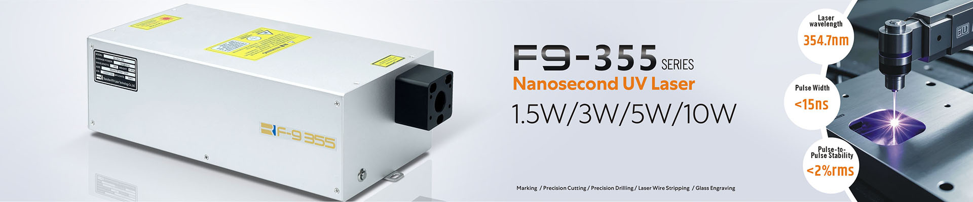
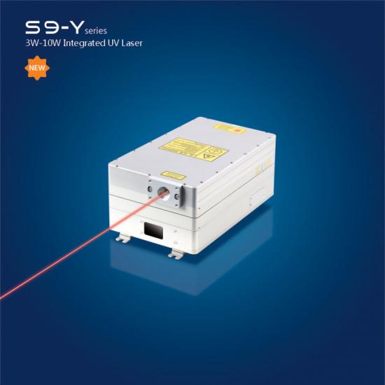
3W-10W S9 Pulsed Ultraviolet Solid State Laser-2020 New Products
product description
According to the needs of market development, the S9 series pulsed ultraviolet solid-state laser newly launched by Shenzhen Ruifengheng Laser Technology Co., Ltd. in 2020 is smaller in size, more refined in design, and more stable in light output than similar products. The small and compact design means that users do not need to make a large optical path, which can greatly reduce costs and save space, and can be easily installed in the field of flying marking equipment. The S9 UV laser is not only small in size, but also has a more stable cavity structure and stronger expansibility than similar products. The same cavity can generate lasers of various powers, and the stability of different power segments is greatly improved.
Product Features
Small size, high precision, high stability
solution
Provide solutions specifically for the field of flying assembly line marking
Application field
Consumer Electronics/Semiconductor/PCB/Medical/Lithium Battery/Automotive Electronics/Industrial Electronics
Product 2 35W Green Laser
product description
The Expert III 532 series water-cooled green semiconductor-pumped pulsed solid-state laser developed and produced by Shenzhen Ruifengheng Laser Technology Co., Ltd. has a power of 35W. This series of lasers is especially suitable for surface processing of most metal and non-metal materials such as glass marking, thin film etching, metal oxide layer breaking, etc. High power, high precision, high stability
Product Features
High power, high precision, high stability
solution
Provide high-power PCB cutting, glass engraving solutions
Application field
Consumer Electronics/Semiconductor/PCB/Medical/Lithium Battery/Automotive Electronics/Industrial Electronics
product description
■ Strong and reliable, long service life
■ Lightweight design
■ Repetition frequency 0-500kHz, stable high power output at high repetition frequency
■ Excellent beam quality
Applications
PCB/FPC, glass, wafers, solar cells, specific metal materials
Product 1 Industrial Pseudo-Coaxial Vision Galvo
Product Features
■ Template dynamic positioning to adjust the position of marking graphics (calibration of mark points)
■ Image outline extraction and marking
■ Image capture and partial image marking
■ Any angle, any quantity, automatic identification of the product to accurately mark the designated position
■ Small distortion lens, small distortion to avoid calibration.
■ Can be used with lasers of various wavelengths such as fiber, CO2, ultraviolet, green light, etc.
Application field
Consumer Electronics/PCB/Automotive Electronics/Industrial Electronics
Product 2 Industrial Rangefinder Vision Galvo
Product Features
■ Template dynamic positioning to adjust the position of marking graphics (calibration of mark points)
■ Image outline extraction and marking
■ Image capture and partial image marking
■ Visual marking, marking size, range and position are visible
■ Any angle, any quantity, automatic identification of the product to accurately mark the designated position
■ Support automatic fine correction of galvanometer
■ Can be used with lasers of various wavelengths such as fiber, CO2, ultraviolet, green light, etc.
Application field
Consumer Electronics/PCB/Medical/Lithium Battery/Automotive Electronics/Industrial Electronics
solution
Laser marking has become an important processing method in modern manufacturing, especially in the fields of precision machining and micromachining. Laser marking is a marking method that uses a high-energy-density laser to irradiate a certain part of the workpiece to vaporize or change the color of the surface material, thereby leaving a permanent mark. Laser marking can print various characters, symbols and patterns, etc., and the character size can range from millimeters to micrometers, which is of special significance to the anti-counterfeiting of products. The very fine laser light speed after focusing is like a tool, which can remove the material on the surface of the object point by point. Its advanced nature is that the marking process is non-contact processing, which does not generate mechanical extrusion or mechanical stress, so it will not damage the processed items; And because the laser focused size is small, the heat-affected area is small, and the processing is fine, some processes that cannot be achieved by conventional methods can be completed.
Traditional laser marking machines generally do not have the function of detecting the position of the workpiece, and use fixtures to achieve positioning, that is, manual intervention and positioning. However, it is very difficult to achieve precise positioning when marking fine or extremely small processing objects, and it is difficult to pick and place the processing objects. In addition to human factors, it is difficult to ensure the accuracy and consistency of the marking position in actual operation. sex. The positioning of the product processing by the accuracy of the fixture will directly affect the marking position accuracy of the parts, and the coordinate position of each processing object is unique. At the same time, the marking effect of processing objects below the millimeter level cannot be distinguished by the naked eye, and an independent detection system is required to detect, and manual intervention and positioning are cumbersome, the degree of automation is low, and the accuracy is difficult to effectively guarantee.


