Latest Blog
355nm UV laser cutting ceramic circuit boards: the pursuit of higher precision
Jul 20 , 2022355nm UV laser cutting ceramic circuit boards: the pursuit of higher precision
With excellent thermal performance and high stability, ceramic circuit boards are ideal for extreme conditions and are widely used in various application scenarios such as automotive, aerospace, 3C consumer electronics, communications, and medical.
A coin always has two sides, and so do ceramic circuit boards. Although the performance of ceramic circuit boards is very superior, its high hardness and brittleness require high processing equipment, and it is difficult to form and process. It is impossible to obtain high precision by using traditional mechanical processes such as milling, sawing, and drill drilling. The quality of cutting and punching, not to mention meeting the current trend of small component size, high density and multi-layered circuit boards, as well as the needs of various small-diameter through holes and blind holes.
uv laser | green laser | Ultraviolet lasers | uv dpss laser | nanosecond laser | UV laser source | Solid State Lasers
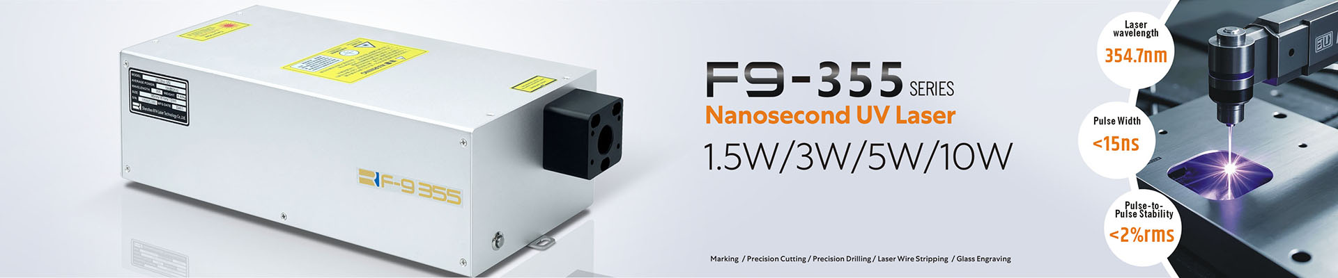
Lasers have gradually replaced traditional machining processes due to their very high power density and collimation. In the processing of ceramic circuit boards, the 355nm ultraviolet laser beam output by the RFH 355nm ultraviolet nanosecond pulse laser is focused and acts on the ceramic surface. The extremely high power density can melt and vaporize the ceramic material, and finally realize cutting according to the process needs. Divide the board or form through holes and blind holes. Especially for the high hardness and brittleness of ceramics, we can make use of advantages and avoid disadvantages, so as to obtain good processing results and high processing efficiency:
Compared with the traditional machining process, the non-contact machining can avoid mechanical stress acting on the hard and brittle ceramic sheets, avoid cracks and lead to defective products, or affect the use effect of ceramic circuit boards;
355nm UV light is easy to focus, and the beam quality of this laser is excellent (M2<1.2), and the focused spot diameter can reach 10-20 microns, which has great advantages in cutting and micro-hole processing, and the cutting line width is small , the hole diameter is small, which can save product consumables;
The cold light source characteristics of 355nm ultraviolet light, with a pulse width of about 20ns, the thermal influence range is very small, and the influence of heat on the incision can be avoided during cutting, and the edge of the processing area is smoother and neater, with less chipping;
The highly repeatable performance of the laser brings large-scale and batch processing, which meets the development requirements of a large number of circuit boards, high density and high precision.


