Latest Blog
Application of 355nm Ultraviolet Laser in Fine Processing of Single Crystal Silicon
Jul 20 , 2022Application of 355nm Ultraviolet Laser in Fine Processing of Single Crystal Silicon
Monocrystalline silicon is widely used in precision devices, semiconductors, photovoltaics and other industries, but it is not easy to process monocrystalline silicon with high precision and high quality. This is because monocrystalline silicon is a typical covalently bonded material. It has high hardness and brittleness. When using traditional emery wheel and other methods for cutting, the mechanical stress applied to the surface of single crystal silicon will easily lead to large kerf chipping and micro-cracks, resulting in a decrease in product yield.
In recent years, the use of lasers for material processing has become increasingly common. For example, visible light or infrared light is used to focus on the focal point, and heat is used to melt the material, and this heat treatment processing method has a very large heat-affected zone, which is suitable for processing at the macro level.
uv laser | green laser | Ultraviolet lasers | uv dpss laser | nanosecond laser | UV laser source | Solid State Lasers
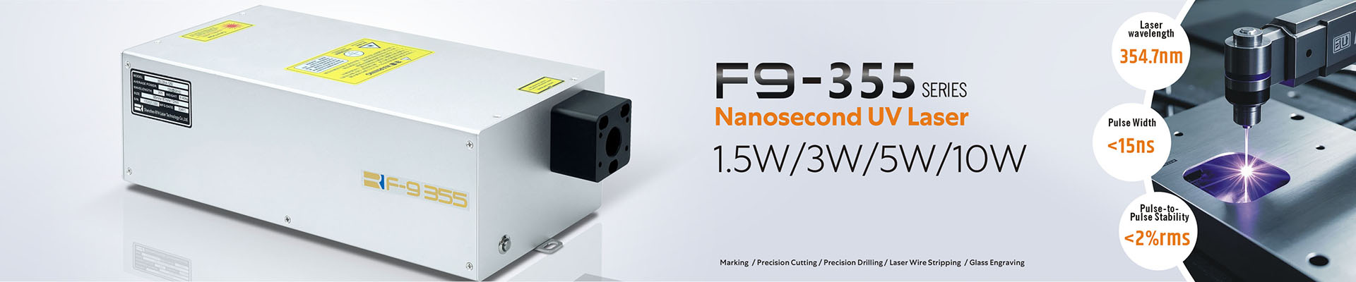
The use of 355nm ultraviolet nano-pulse laser can perform fine micro-processing at the microscopic level, and can obtain high processing quality. This is due to the advantages of short wavelength, high material absorption rate, small spot size, easy focusing, high single-photon energy, and high beam quality of the 355nm ultraviolet laser, which avoids thermal defects and deficiencies caused by visible light or infrared laser processing. In addition to the fine processing of polymers, films and other materials, it can also perform high-precision cutting, scribing and drilling operations on hard and brittle materials such as single crystal silicon, sapphire, and glass. It has the characteristics of fast processing speed and small heat affected zone. . In addition, the medium and high power 355nm ultraviolet laser can increase the writing rate and reduce the influence of the material surface on the etching in the laser etching and deposition of single crystal silicon solar panels.
Based on the broad market and application prospects of the 355nm UV laser, RFH has designed a 355nm UV nanosecond solid-state laser with independent intellectual property rights. The power is optional from 5W to 15W and 20W, which can meet the requirements of precision cutting, Punching and etching, etc. Its beam quality is high (M2<1.2), the diameter of the focused spot is only 10-20um, and it can process and cut or scribe tiny parts. The line width is very narrow, and the utilization rate of single crystal silicon material is very high. When punching, it is also easy to obtain holes with a size of tens of microns, and the hole walls are smooth.
At the same time, its pulse width is only about 20ns, and the heat is often accumulated before the material is processed, which brings a smaller heat-affected zone, which is of great significance in fine processing.


