532nm green laser etching PCB circuit board
Nov 10 , 2022532nm green laser etching PCB circuit board
The copper clad laminate is the basic material of the PCB. In the traditional production process of the PCB, the processing technology mainly removes the copper clad layer except for the wiring diagram on the copper clad plate by chemical etching, and additional steps such as cleaning and degumming are added, not to mention For other processes such as drilling, hole metallization, and coating in the middle, the whole process has a long process cycle, and is limited by the reticle, resulting in low precision and easy environmental pollution.
With the development of PCB boards from single-sided to double-sided, from single-layer to multi-layer, there are rigid boards, flexible boards and rigid-flex boards, and they are constantly developing towards high precision, high density, high reliability and high performance. It is also getting smaller and smaller, and the fineness and production capacity of the traditional manufacturing process are obviously insufficient, which is not conducive to mass processing and production.
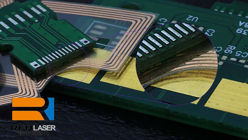
Laser processing gradually replaces traditional processing technology with high efficiency, high consistency and high precision, and also has important applications in PCB circuit etching. The 532nm green laser can be used to directly complete the etching without a mask, and it can be done in one step, avoiding the pollution and cumbersome operations of the traditional chemical etching method. The processing mechanism is to act on the copper layer of the copper clad laminate by a high-energy density laser beam, so that it can be quickly evaporated and vaporized to achieve the purpose of removal, so as to produce the required circuit pattern.
The excellent beam quality (M2<1.2) and the easy focusing characteristics of the 532nm green laser make the spot size of the output laser beam in the order of microns, which can match the processing requirements of complex PCB boards and fine circuits, bringing higher processing. ; High stability can keep the etching quality more consistent and the appearance is good. At the same time, the single-photon energy of the 532nm green laser is high, and the copper material has a good absorption peak in the 355nm band compared to other bands, supplemented by a narrow pulse width of about 25ns, the thermal effect during processing is small, and the heat affected zone is small, even if the In the face of flexible circuit boards (FPC) based on materials with high thermal sensitivity such as PI film, it also has a very good processing effect, and the "cold" processing effect is worthy of the name.

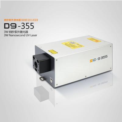
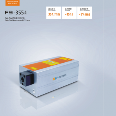
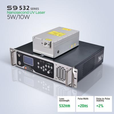
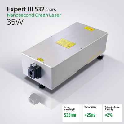
About Expert III 532 Green Laser 35W: https://www.rfhtech.com/expert-iii-532-green-laser-35w_p16.html
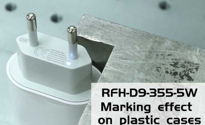
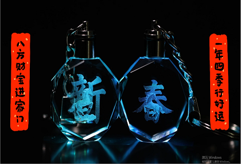
Today, 532nm green lasers are widely used in circuit board manufacturing. Different powers have different divisions of labor. For example, low power of 3-5W can be used for high-quality marking of PCB boards or FPC flexible boards, and higher power can be used for punching holes. (through holes or blind holes), cutting, etc., are reliable tools for improving quality and efficiency in the production process of circuit boards.