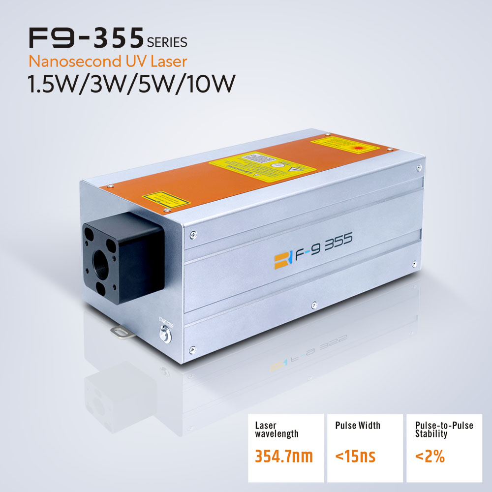
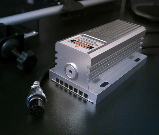
Selective Material Removal by high power 355nm DPSS Pulsed Nanosecond uv Lasers
Jan 06 , 2023Selective Material Removal by high power 355nm DPSS Pulsed Nanosecond uv Lasers
Within the microelectronic, medical device, automotive and aerospace industries, definition of conductor paths or removal of insulation are common requirements. Thin coatings of materials; typically polymers, are used to provide electrical insulation, biocompatibility or harsh environment protection for advanced technology devices. These protective materials usually adhere and conform to the 3-dimensional parts they are protecting, and the typical application techniques provide very little opportunity to leave areas of the part un-coated. Historically, the most common approach to removing areas of coating has been to apply a physical mask in the form of a tape or film prior to coating, or to define the shape perimeter with a blade and then peel off the coating as a post-processing step. More recently, laser systems offering fast, efficient and highly precise alternative methods that produce high part quality have become available.
Similarly, thin coatings of conducting materials, typically gold, alloys and ITO are used to provide electrical connections. Selective removal of these films to provide electrical isolation, or to define a particular circuit
path is a common manufacturing process. Laser systems are not only a fast and efficient production technique, they offer the flexibility to modify pattern shape and circuit design by a simple change to the processing program, eliminating the need for slow and costly changes to mask and tool sets.
In both applications, avoiding any damage to the underlying substrate as the top material is removed is a critical requirement. Because materials behave differently with various laser parameters (wavelength, pulse energy, pulse duration, fluence, repetition rate etc.), careful selection of laser type and operating conditions is required.
Application Labs boast an outstanding team of Ph.D. material scientists devoted to optimizing these processes.
UV Ablation and fully automated Polymer Film Cutter high volume production systems are ideal micromachining workstations for selective material removal.
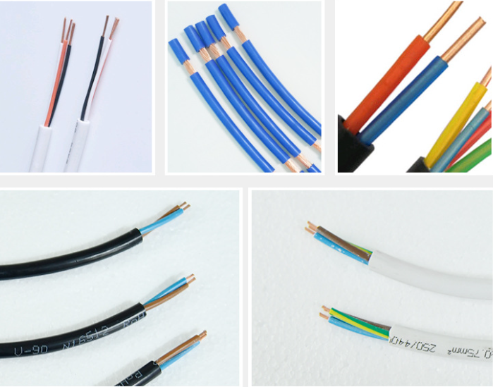
Wire Stripping Polymer from Wire Core
A low energy uv laser source is used to selectively ablate coating from bulk material. In situations where the coating ablates at a lower energy density than the base material, damage to the bulk material is avoided. Typical part alignment is better than 5 µm, enabling highly accurate coasting removal.
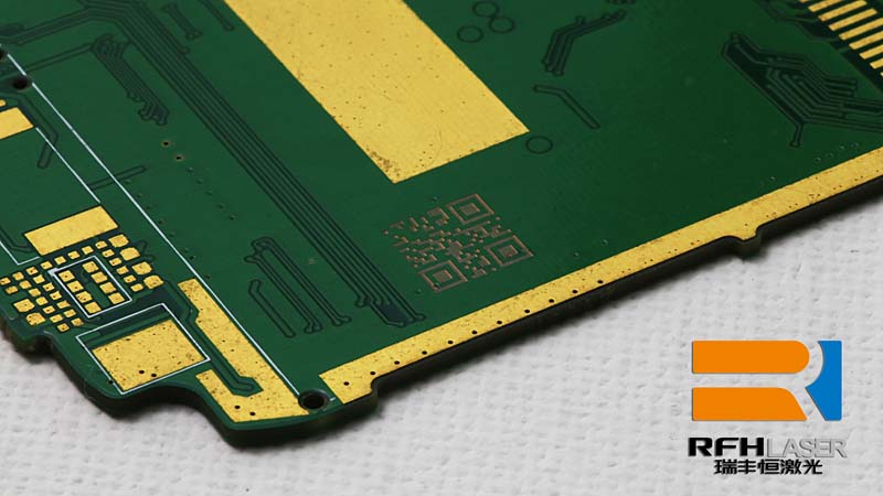
Parylene Removal for Printed Circuit Boards
Parylene and other conformal coatings are readily removed from electronic circuit boards and other components without damage to delicate wire bond pads or part features. Alignment is better than 5 µm, with manual load and fully automated operation options available.
CdTe Removal from Glass Solar Panel
Selective material removal combined with laser lift-off process technology enables removal of single layers from multi-layer structures, such as CdTe thin film from glass / ITO substrate solar panels.
Precision scribe alignment to <20 µm
Patterning Gold on PET
High-quality laser direct patterning of isolation path in 50nm thick gold conductor on PET substrate. Pulse length and energy density optimized to produce metal removal with no damage to the underlying polymer
Metal Patterning Film on Glass
Patterning of thin films by direct material UV ablation.
Minimum feature sizes typically 10 microns.
Figure shows Laser Patterned Gold on Glass.
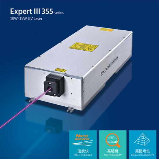
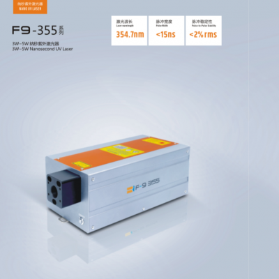
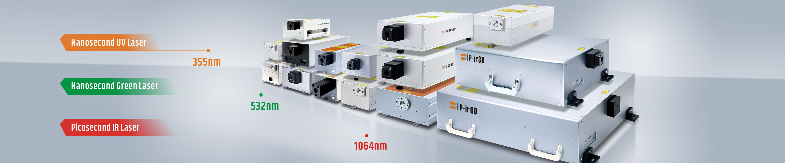
what is 355nm uv laser: https://www.rfhtech.com/expert-iii-355-high-power-uv-laser_c7