Latest Blog
355nm UV nanosecond laser marking electronic circuit board logo, date, graphic
Aug 15 , 2022355nm UV nanosecond laser marking electronic circuit board logo, date, graphic
Laser marking has a wide range of penetration in the field of electronic manufacturing, from common PCBs and FPCs to capacitors, resistors, memory, chips, etc. on circuit boards. Laser marking is used to obtain high-quality, high-contrast, high-efficiency logos and numbers. , production date, assembly line, warehouse and other graphic marks are not uncommon.
Compared with traditional screen printing technology and traditional marking methods such as labeling, laser marking is incomparable with its fast marking speed, environmental protection, strong firmness, anti-counterfeiting traceability and flexible operation. In view of the development trend of electronic components towards precision, refinement and batchization, when marking electronic components with 355nm ultraviolet nanosecond laser, it also has the characteristics of "cold" processing, high marking resolution and narrow line width. The realization of these characteristics is inseparable from the key data of the laser itself.
355nm UV light - "cold" processing. 355nm ultraviolet light can be absorbed by most metal and non-metal materials, and the wavelength is short, and the single photon energy is higher. When 355nm ultraviolet light is used for marking, it can easily break the molecular bonds of the material and separate the surface molecules from the material. This process does not generate high heat, so it is called "cold" processing. For soft and hard circuit boards and component materials commonly used in electronic manufacturing, 355nm ultraviolet light is friendly.
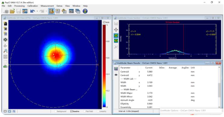
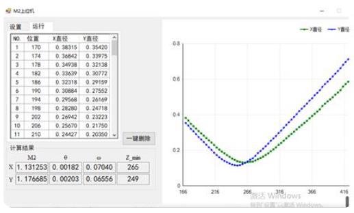
Excellent beam quality - high resolution, narrow linewidth. As the components are getting smaller and smaller, the area that can be marked is becoming more and more limited, 355nm ultraviolet light is easy to focus, and the laser beam quality is high (M2 < 1.2), the focused spot diameter is micron, and the marking line width can be 0.08 to 0.2mm, so it is possible to mark images and texts less than 1mm on the surface of components. The extremely fine light spot is more advantageous in marking the QR code. The resolution of the marked QR code is very high, which can be easily scanned and identified. At the same time, manufacturers can use the QR code to achieve product traceability and anti-counterfeiting functions.
In addition, the high flexibility and non-contact processing of laser marking also fully enables electronic manufacturing. On the one hand, the high flexibility is reflected in that the graphic and text marks can be changed at will through the drawing software, and the serial number variable that can be jumped, the date and time variable that can be changed with the system standard time, etc. can be flexibly set. It can also be uniformly marked; the advantage of non-contact processing is that it does not generate mechanical stress, so that components are free from pressure and damage, which in turn affects the usability and safety of products and improves the yield.


