Latest Blog
An article to understand what is UV DPSS Laser Source
Jun 21 , 2022An article to understand what is UV DPSS Laser Source
1 Introduction
With the rapid development of science and technology, more portable, efficient, miniaturized, multi-functional and high-quality laser instruments and equipment are required in electronics, medical treatment, biology and materials. At present, the wavelengths of common lasers are infrared and visible light. Traditional laser tools, processes and technologies have problems such as low efficiency, complex operation, high cost, limited range, serious loss, and low accuracy. In recent decades, ultraviolet lasers have been repeatedly researched and breakthroughs by scientists because of their relatively high coherence, more convenience, stability and reliability, low cost, tunability, small size, high efficiency, high precision and practicality.
2. Ultraviolet Laser
Ultraviolet lasers are mainly divided into gas ultraviolet lasers and solid ultraviolet solid-state lasers. Under the action of the pump source, the working medium reaches the excited state by absorbing the external energy. After the population inversion, the gain is greater than the loss, and the light is amplified. Part of the amplified light feedback continues to be excited to generate oscillation in the resonant cavity to generate laser light. The gas medium mainly uses pulse or electron beam discharge, and the gas particles are excited from the low energy level to the high energy level through the collision between electrons to generate excited transitions to obtain ultraviolet laser light. The solid medium is a non-linear frequency-doubling crystal to generate an ultraviolet laser that radiates outward after one or more frequency conversions. Excimer and all-solid-state UV lasers are commonly used in laser processing and processing [1]. The classification of UV lasers is shown in Table 1.
2.1. Excimer Lasers
Gas UV lasers mainly include excimer lasers, argon ion lasers, nitrogen molecular lasers, fluorine molecular lasers, helium-cadmium lasers, etc. Excimer lasers etc. are commonly used for laser processing [2]. Excimer laser is a gas laser with excimer as the working substance. It is also a pulsed laser. Since the birth of the first excimer laser in 1971 [3], it has great research significance. An excimer is an unstable compound molecule that breaks down into atoms under certain circumstances. Repetition frequency and average power are the criteria for judging excimer lasers. A certain proportion of Ar, Kr, Xe and other rare gases mixed with F, Cl, Br and other halogen elements are the main working substances of ultraviolet gas lasers. The pumping method is achieved by electron beam or pulse discharge. After the noble gas atoms and rare gas atoms in the ground state are excited, the extranuclear electrons are excited to a higher orbit, so that the outermost electron layer is filled, and combined with other atoms to form excimers, which then transition back to the ground state and then decompose into The original atom and the remaining energy are separated in the form of photons and finally the ultraviolet laser is obtained through the amplification of the resonant cavity, as shown in Fig. 1 [1]. Liquid xenon was the working substance of early excimer lasers. Excimer lasers now include ArF lasers at 193 nm, KrF lasers at 248 nm, and XeCl lasers at 308 nm.
2.2. Solid-state UV lasers
The outstanding advantages of all-solid-state UV lasers are convenience, small size, high reliability and stable operation. The most commonly used Nd:YAG crystal is used for LD pumping, and then frequency doubling is shown in Figure 2 [4].
The main steps of generating UV solid-state lasers are: firstly, the pump light source in the laser is irradiated on the reinforcing medium to achieve population inversion [5], the fundamental red light is formed and oscillated in the resonator, and then passes through one or more nonlinear nonlinearities. Frequency doubling in the crystal cavity, after transmission and reflection, the desired ultraviolet laser is finally output from the resonant cavity. Ultraviolet solid-state lasers are usually obtained by LD diode pumping and lamp pumping. The all-solid-state UV laser is an LD-pumped UV solid-state laser, and its optical circuit principle is shown in Figure 3 [1].
Nd:YAG (neodymium-doped yttrium aluminum garnet) and Nd:YVO4 (neodymium-doped yttrium vanadate) are two of the more common reinforcement dielectric crystals. The commonly used method to enhance the resonant cavity is to use a small semiconductor laser diode LD with a wavelength of 808 nm to pump a Nd:YVO4 laser crystal to generate near-infrared light at 1064 nm, and frequency doubling in the cavity to output a green light with a wavelength of 532 nm, which is then fed into the enhanced cavity. The resonator frequency quadruples, the output wavelength of deep ultraviolet laser is 266nm, and the input threshold of fundamental frequency green light can be as low as 215 mW [6]. Compared with Nd:YAG, Nd:YVO4 laser crystal has a larger gain cross-section, which is 4 times that of Nd:YAG; the absorption coefficient is large, which is 5 times that of Nd:YAG, and has the advantages of low laser threshold. Nd:YAG crystal has relatively high mechanical strength, high light transmittance, long fluorescent life, and does not require an excessively severe cooling system. At present, UV solid-state lasers are usually used at home and abroad, and Nd:YAG crystal is selected as the gain medium.
3. Application of UV Laser
Ultraviolet laser processing has many advantages, and it is also the preferred technology in the development of scientific and technological information. First, the ultraviolet laser can output ultra-short wavelength laser light, which can accurately process ultra-small and fine materials; secondly, the "cold treatment" of the ultraviolet laser will not destroy the material itself as a whole, but only treat the surface; and basically no thermal damage is affected [7] ; Some materials cannot effectively absorb visible light and infrared lasers and cannot be processed. The biggest advantage of ultraviolet is that basically all materials have a wide range of ultraviolet light absorption [8]. Ultraviolet lasers, especially solid-state ultraviolet lasers, are compact in structure, small in size, easy to maintain, and easy to mass-produce. Ultraviolet lasers are widely used in processing medical biological materials, forensics in criminal cases, integrated circuit boards, semiconductor industry, low-light components, surgery [9], communications and radar, and laser processing and cutting.
3.1. Changing the surface properties of biomaterials
In some treatments, many medical materials need to be compatible with human tissues, or even repaired, such as ultraviolet laser treatment of intraocular diseases [10] and rabbit cornea experiments [11] Sometimes it is necessary to change the properties of biological proteins [12] and biological macromolecules Molecular structure [13], adjust the optimal pulse parameters of the excimer UV laser, the experimenters then use 100 nm, 120 nm, 200 nm laser to irradiate the surface of the medical biological material respectively, so as to improve the physical and chemical structure of the material surface without changing the The overall chemical structure of the material, through the comparative experiment of cultured biological cells, significantly improves the compatibility and hydrophilicity of the processed organic biological material with human tissue, which is of great help in medical biological applications [14].
3.2. Criminal investigation
In the field of criminal investigation, when it is found that fingerprints have the same unique characteristics as DNA, fingerprints can be used as important biological evidence left at the crime scene by criminal suspects. The once-old method resulted in sample damage, making collection and storage of evidence difficult. The current research has outstanding effects on the surface fingerprints of non-permeable objects, such as tapes, photos, and glass. "Ultraviolet luminescence imaging technology" and "ultraviolet laser reflection imaging technology" means that the ultraviolet laser with a wavelength of 266 nm irradiates the latent fingerprint, and passes through the bandpass filters of 266 nm and 340 nm respectively to observe and record the ultraviolet laser on the fingerprint. Detection and adoption collection [15]. Seventy percent of the 120 experimental samples in the experiment were successfully detected. Ultraviolet short-wave technology improves the success rate of potential fingerprints, and it is convenient, quick and easy to control its optical properties, and has broad application prospects in the field of forensic science. UV detection can be used for the detection of common biological materials such as saliva spots, exfoliated cells, blood stains, and hair with follicles. However, the short-wavelength 266 nm ultraviolet laser was used to irradiate the biological samples at a fixed distance and for different lengths of time to extract DNA for analysis. It was found that the short-wavelength 266 nm ultraviolet laser had five common types of fingerprints, blood stains, saliva spots, shed cells, and hair with follicles. The DNA test results of biological evidence have a serious impact, but the detection of biological DNA for hair, including hair follicles, bodily fluids, saliva, and blood stains, has only a small impact. Short-wave ultraviolet laser will affect some DNA biological samples, so the extraction method should be carefully selected according to the role of evidence in criminal investigation and evidence collection [16].
3.3. Application of UV laser on integrated circuit board
In the production process of various circuit boards in the industrial field, from the initial wiring to the production of tiny and precise embedded chips that require advanced technology, flexible circuits, polymer and copper layered circuits in integrated circuit boards are all Micro-hole drilling and cutting are required [17], as well as repair and inspection of materials on circuit boards, which often require micromachining and processing. Laser micromachining technology is obviously the best choice in circuit board processing. In the process of laser processing, the working machine does not contact the processed product, effectively avoiding mechanical force, processing fast, high flexibility, and no special requirements for the workplace. Through the precise setting and research and design of laser parameters, the micron of the following magnitude [18]. The more traditional drilling method used on circuit boards is to use UV lasers and CO2 lasers for non-metallic marking (CO2 lasers with a wavelength of 10.6 μm are used for non-metallic material marking; wavelengths of 1064 nm or 532 nm are generally used for metals. material marking [19]). At present, ultraviolet laser processing technology is mainly used, which can achieve micron-level processing, with high precision, can make ultra-fine zero devices, and can be applied to micro-hole processing of laser beams with a spot smaller than 1 μm. However, the CO2 laser mainly punches 75-150 mm holes, and the small holes are easy to be dislocated, while the UV laser can punch holes below 25 mm with high precision and no dislocation [20]. For example, in the "cold" processing of copper clad circuit boards with ultraviolet femtosecond lasers, the comprehensive balance method is used to obtain the optimal process parameters, and then the characteristics of selective etching are used to achieve high-quality, high-efficiency line widths of 50 μm and line spacing of 20 μm. Figure 4 and Figure 5 show the etching process of fine lines on the surface of CCL [21].
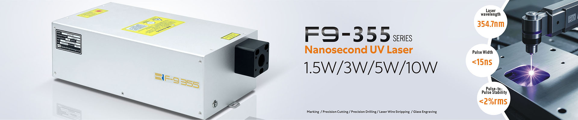
uv laser | green laser | Ultraviolet lasers | uv dpss laser | nanosecond laser | UV laser source | Solid State Lasers
3.4. Processing and preparation of low-light components
In the information age of the rapid development of science and technology and modern industry, in order to build more experimental systems and realize more functions in a smaller space, it is necessary to speed up the development of information technology. More importantly, it is necessary to produce and process more A fully functional device that is miniaturized, miniaturized, and only handles chemical bonds on the surface of the material [22]. It has important application and research value in the fields of military radar communication [23], medical treatment, aerospace and biochemistry. It is possible to carry out more in-depth cutting and optimization on nano-scale micro-optical components and research and develop applications, transforming the functions and characteristics of traditional optical components. Micro-optical elements have the advantages of easy mass production, easy arraying, compactness, lightness and flexibility, but their main material is quartz glass. Quartz glass is prone to cracks and pits during application and handling, and is a hard and brittle material, which greatly reduces its optical properties. Therefore, the direct writing "cold" processing technology of UV laser [24] greatly improves the efficiency of micro-optical devices, quickly completes the processing of micro-optical components with high precision and microstructure without damaging the material, and can flexibly complete the processing of different needs of large and small batches. processing. The research on UV-UV processing of silicon wafers by foreign scientific research institutions is relatively early [25], and the research on the cutting technology and section of silicon wafers started later in China [26]. More than ten years ago, Zhang Fei and others used the UV all-solid-state laser developed by themselves to study the micromachining system, and optimized the cutting of three silicon wafers of the same material (0.18 mm, 0.38 mm, 0.6 mm), with a minimum aperture of 45 mm. μm, the machining accuracy is 20 μm, the results show that there is no crack in the material, the thermal influence of the laser is small, and the spatter is less [27], as shown in Figure 6.
3.5. Application of UV Laser in Semiconductor Industry
In recent years, the micromachining of semiconductor materials by UV laser has received more and more attention. Thousands of dense circuit components are very common in integrated circuits, so some high-precision processing and processing methods are required [28], and there are also some high-precision instruments and devices for semiconductor materials such as silicon and sapphire. Micromachining relies on ultraviolet lasers and studies the spectral properties of thin films [29]. At the same time, ultraviolet lasers can also increase the utilization rate of light energy by silicon materials, and can also change the microstructure of the silicon surface, which is beneficial to the research and development of solar panels. Such as two-dimensional micro-grating and so on.
In 2018, Li Qisi et al. used a 355 nm all-solid-state ultraviolet laser to study the surface and engraving depth, bottom surface smoothness, and channel verticality of borosilicate glass, and experimentally analyzed and optimized the processing parameters. , The vertical and flat borosilicate glass microchannel [30] is shown in Figure 7.
4 Conclusion
Through these decades of development and research, the technology and application of UV lasers have become more and more extensive and mature. Its most characteristic fine "cold" processing technology can micro-process and treat the surface without changing the physical properties of the object. , widely used in communications, optics, military, criminal investigation, medical and other industries and fields. For example, the 5G era has spawned the market demand for FPC processing. With the further development of the 5G industry and the pursuit of flexible OLED displays by major electronic product manufacturers, the market demand for FPC flexible circuit boards has grown rapidly, and the demand for ultraviolet lasers will also grow rapidly. . This development trend is expected to rapidly promote the development of UV technology itself, to achieve greater breakthroughs in power and pulse width, and to expand more new application fields. The application of ultraviolet laser machines makes it possible to perform precise cold processing of FPC and other materials, and the gradual increase of FPC has promoted the deployment of 5G. The low-latency characteristics of 5G have brought a new wave of technologies such as cloud technology, Internet of Things, unmanned driving, and VR. The technological development provides infinite vitality. Of course, this is a complementary concept, and new technologies and new applications will eventually drive the further development of UV lasers.
With the emergence of more and more new frequency-doubling crystals and gain media, ultraviolet lasers with shorter wavelengths and higher power will be used in more industries in the future, promoting the development of all walks of life. Intelligence, high efficiency and precision, high repetition rate and high stability are the trends of future development.


