The Advantages of high power UV Laser-Based PCB Cutting Depaneling
Feb 07 , 2023The Advantages of high power UV Laser-Based PCB Cutting Depaneling
Technological changes in the materials, thickness, and composition of PCBs are motivating a
move away from traditional mechanical cutting and depaneling methods towards laser-based
processes. But not all lasers for PCB depaneling are created equal. There are significant
differences amongst various lasers in cut characteristics and quality, specifically in terms of
heat affected zone (HAZ). This, in turn, affects process utilization since it determines how
closely circuits can be placed on a PCB, and can also impact circuit functionality and
downstream processes like waterproofing or EMI shielding. This document presents a new
nanosecond laser and associated cutting process developed at Coherent Inc. which enables
laser PCB depaneling with substantially reduced HAZ compared to other currently available
products.
The Evolving Need for Laser Depaneling
The continued market growth of miniaturized electronic devices, including smartphones,
various wearables, VR devices, automotive sensors, and home automation equipment, to name
just a few examples, translates directly into a need for denser, higher performance PCBs. Not
only are these devices physically smaller and more complex than the previous generation of
microelectronics, there is also a consumer demand for to make them more energy efficient (for
longer battery lifetime) and less expensive.
In terms of PCB technology, this has driven several trends. Amongst these are the use of
thinner traditional boards, wide scale implementation of flex circuitry, thicker conductive layers,
and increased utilization of low-κ dielectrics (the latter especially for 5G technology). Cost
considerations also prompt a need for improved process utilization. Specifically, this translates
into placing boards closer together on a panel to increase yield.
In terms of depaneling, all this necessitates increasingly narrow kerf widths and higher
dimensional accuracy for the cutting process. Closer physical proximity of the cut to the
functional areas of the PCB also means that the cutting process must not affect the
surrounding material or circuitry, whether due to mechanical stress or heat. Minimal
production of debris, which might require a subsequent cleaning step, is another requirement.
All these constraints make traditional mechanical PCB depaneling methods, including routers,
saws, die cutting, punching, scoring, and pizza cutting, etc., less practical and less cost effective.
This impels a move towards laser cutting which offers substantial benefits in virtually every one
of the areas previously mentioned, although usually at the expense of reduced cutting speed.
Understanding Laser Cutting
Laser depaneling has, of course, been in use for some time. However, it’s important to
understand and differentiate between the various laser-based technologies. The original
implementations utilized CO2 lasers which emit in the far infrared. This technology cuts by
heating the bulk material, which results in a significant HAZ. Also, compared with shorter UV
wavelengths, this long wavelength cannot be focused to as small a spot size, meaning a larger
kerf width.
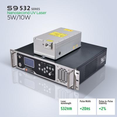
Over a decade ago, the diode-pumped solid-state (DPSS), nanosecond pulsewidth, frequencytripled laser emerged as a viable source for PCB depaneling. It offers ultraviolet (355 nm)
output with sufficient pulse energy to enable material removal through a relatively “cold”
ablation process. That is, one with a much smaller (but still noticeable) HAZ than the CO2 laser,
and also substantially less production of debris and recast material. The pulse energy and
repetition rate of commercially available sources enable cutting at economically viable feed
rates, although not as fast as the CO2 laser. The primary benefits of this technology are
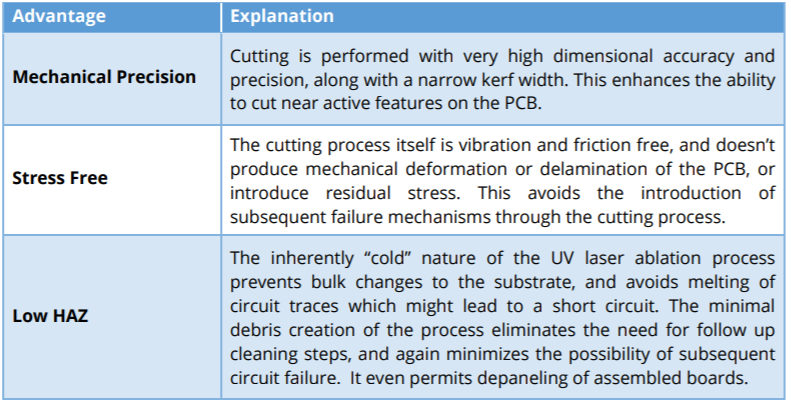
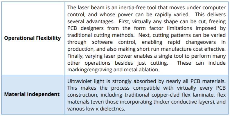
summarized in the table.
Table 1. Primary Characteristics and Advantages of UV Laser-Based PCB Cutting
While laser depaneling clearly delivers numerous benefits, PCB manufacturers are already
pushing this technology to the limits in order to meet the ever more stringent size, materials,
and cost challenges presented by the market forces mentioned at the outset. In particular,
achieving further reductions in HAZ and debris formation, and improving the cut quality
obtained with nanosecond pulsewidth UV DPSS lasers, is an active area of development.
To aid in this effort, applications research at Coherent Inc. has explored the outcomes and
process space of using a nanosecond pulsewidth, high pulse energy, UV DPSS laser (AVIA LX) for
cutting a variety of PCB materials and material combinations. Based on this work, the Coherent
team developed a new PCB cutting method that has already proven to deliver a reduced HAZ, a
higher quality cut edge, reduced kerf width, and increased production throughput.
One key element of this technique is a proprietary method for controlling the timing and spatial
positioning of laser pulses delivered to the work surface in such a manner that heat buildup is
avoided. Because thermal damage is absent in this approach, it’s possible to utilize a laser with
substantially higher pulse energy when cutting thicker materials (1 mm and above).
The advantage of higher pulse energy is that it eliminates the need to employ the traditional
scheme used for cutting thicker materials. Specifically, this involves making a series of laterally
displaced scribes to produce a “v-groove.” The “v-groove” geometry is necessary in order to
avoid clipping the beam as it penetrates farther into the material when making a high aspect
ratio cut. This would reduce its power, and thus limit ablation efficiency. However, the AVIA LX,
coupled with this novel pulse timing approach, can utilize pulse energies as high as ~400 μJ to
repeatedly scribe along the same line (no lateral displacement, or “v-groove”). The result is
faster cutting and significantly reduced kerf width.
Higher pulse energy also increases the laser focus tolerance at the work surface. Specifically,
when using a lower pulse energy laser, it is necessary to shift the focus of the beam as the
material is penetrated so that the minimum focused spot size is always maintained precisely at
the depth at which cutting is occurring. This is necessary in order to achieve sufficient laser
fluence to get above the material ablation threshold. However, doing this in practice requires
either physically shifting the PCB up, which slows the process, or employing a three-axis
scanner (one which has a focusing capability), which increases equipment cost and complexity.
The higher pulse energy of the AVIA LX makes it possible to simply focus the laser at a point
mid-way through the PCB and perform cutting. This is because there is sufficient laser fluence
for ablation even well out of perfect focus for the laser. The benefit is faster cutting, and
reduced system complexity.
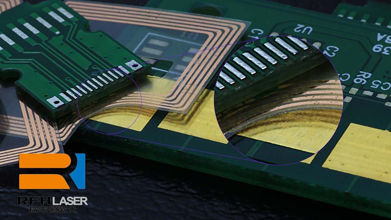
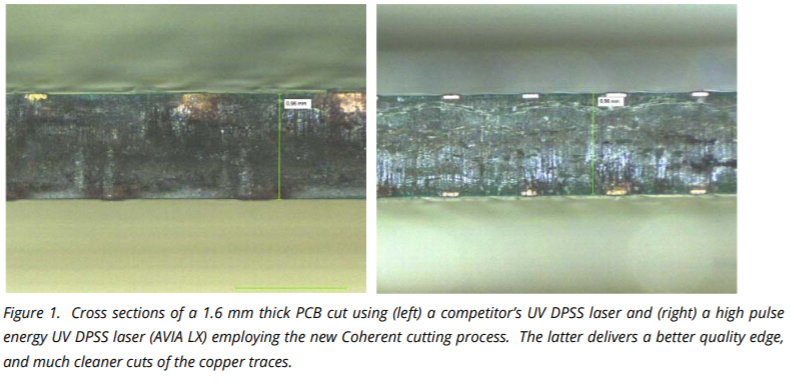
An example of the improvements are shown in the photos below, which compare cuts in a
1.6 mm thick PCB with copper traces, made using the type of UV DPSS laser currently
commercially available for this application versus the same material processed using the AVIA
LX and this new approach. The board processed with this technique shows a cleaner cut edge
and substantial improvement in the cut edges of the copper traces.
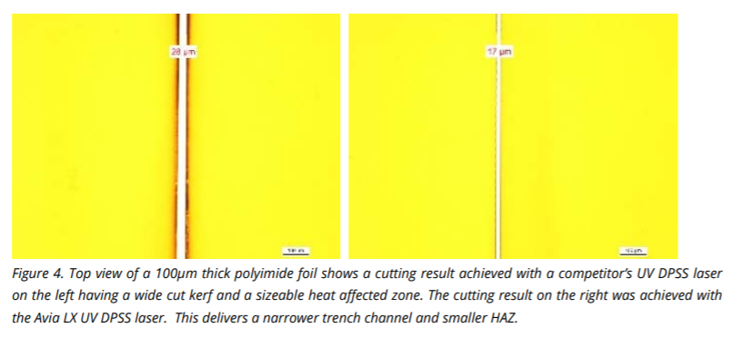
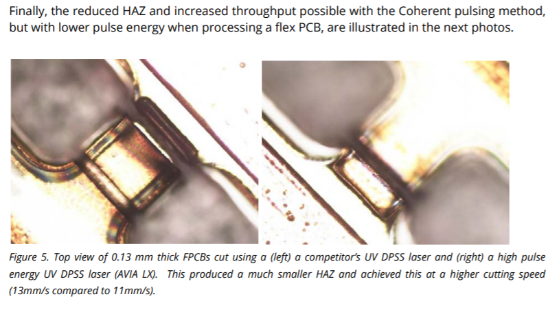
in the past, laser cutting of polyimide and EMI shield foil produced some delamination at the
cut line due to the wide HAZ. In this case, it’s necessary to use lower pulse energy in order to
avoid damaging the material. But, the same pulsing approach is utilized to eliminate heat
buildup, and delivers the same benefits of reduced HAZ and kerf width. This, in turn, reduces
production costs by enabling downstream production processes to achieve higher yields.
Practical, High Pulse Energy DPSS UV Lasers
For traditional thick PCB materials, implementing the Coherent pulse control method in
practice requires a UV DPSS laser source having higher pulse energy than previously
commercially available. To meet this need, Coherent developed the AVIA LX, a 20 W (at 355
nm), solid-state, nanosecond pulsewidth laser, which can produce a pulse energy of up to 500
μJ.
The AVIA LX lase was specifically designed to enable high throughput, high quality PCB
depaneling. It combines a number of technological advances in design and manufacture to
deliver this high energy output along with an unmatched combination of high reliability,
superior performance, and low cost of ownership.
AVIA LX leverages the extensive experience at Coherent in producing reliable, long lifetime
lasers with UV output. The non-linear (frequency tripling) crystals utilized in the AVIA LX are
produced within Coherent, giving us direct control over the quality and optical characteristics of
this critical component, and enabling us to achieve longer lifetime, improved performance and
reduced cost of ownership. Lifetime is further maximized by using a built-in crystal shifter
which contains a map of the actual crystal in the laser, and the location of 20 pre-qualified
third-harmonic generation spots (with over 1000 hours lifetime per spot) within it.
Contamination of the optics is a key limiting factor in the lifetime of UV lasers. AVIA LX lasers
are manufactured in a cleanroom, and the internal optics that are directly exposed to UV light
are contained within a PureUV sealed compartment to prevent contamination in actual use.
This maximizes lifetime and service intervals.
Furthermore, AVIA LX is based on an extremely robust industrial design, which has been
validated by HASS and HALT testing. In HALT (High Accelerated Life Testing), prototypes are
iteratively tested to destruction, re-designed and retested to eliminate any inherent
weaknesses. HASS (Highly Accelerated Stress Screening) then stresses actual production units
beyond their specified operating environment. This protocol screens out any deficiencies in
manufacturing and packaging. The result is unmatched product reliability and lifetime.
AVIA LX is also designed with ease-of-integration and ease-of-use in mind. For instance,
integration is simplified by using built-in control electronics, and an integrated beam expander.
The use of water cooling maximizes lifetime and pulse-to-pulse stability, even when operating
at high power.
In conclusion, the Coherent AVIA LX laser, together with novel pulse control technology, has
demonstrated superior results for PCB depaneling as compared to traditional mechanical
processes, and even previously available nanosecond pulsewidth UV DPSS laser sources. It
should prove a useful source for a variety of the fabrication processes required for next
generation microelectronic devices, including cutting of traditional PCBs and flex circuitry, SiP
cutting and trenching, and EMI shielding cutting.